PETsys TOF DAQ Board
 PETsys TOF DAQ Board PDF
The PETsys TOF DAQ Board is a PCIe data acquisition board that collects data from frontend TOF ASICs in Time Of Flight applications (Fig. 1). Up to four master FEB/D boards (Fig.2) can be connected to the DAQ board using HDMI cables. A master FED/D can be daisy chained with several slave FEB/D boards. Therefore the DAQ board can be integrated with several FEB/D boards forming a complete scalable data acquisition system with tens of thousand channels. Each FEB/D collects data from 16 TOF ASICs in eight FEB/A daughter boards (1024 channels).
The DAQ board receives data frames through four high-speed serial links (1.6 Gbps). The maximum input event rate per FEB/D is 16 M event/s (full event format) or 32 M events/s (compact event format). The maximum out event rate through the PCIe bus is 70 M events/s. Optionally events can be filtered by a coincidence trigger implemented in the board FPGA.
The DAQ board uses four upstream 1.6 Gbps serial links to configure all TOF ASICs in the frontend system.
The DAQ board provides the system clock (80-160 MHz) as well as common synchronization signals that are distributed to all TOF ASICs in the frontend system.
The TOF ASIC (Fig. 3) used in PETsys frontend system is optimized for timing and has 25 ps time resolution (r.m.s.). It uses a low threshold for timing and a high threshold for accepting the event. Both thresholds are separately configurable for each channel. Every time one of the 64 channels exceeds the high threshold a record is created giving the channel number, the time and the amplitude of the event. Activity in one channel does not cause any dead-time on one of the other channels.

Figure 2
Drawing of the FEB/D board.

Figure 1
Picture of the DAQ board.

Figure 3
The 128-channel assembly of two TOF ASICs.
Main features:
- Single PCIe board providing data acquisition of TOF ASICs
- Compatible with FEB/D boards
- Data readout of four master FEB/D boards and associated daisy-chained slaves
- Max total input event rate: 128 M events/s (compact event format)
- Coincidence trigger implemented in the FPGA
- Data output rate 4 Gbps
- Operation frequency 80-160 MHz
- Readout of frontend temperature sensor
- Readout of TOF ASIC dark counters
- Equipped with Virtex4 FPGA
I/O connectors:
The DAQ board has four HDMI connectors carrying the downstream data link, the upstream configuration link, as well as the clock and synchronization lines. All signals are LVDS.
Data frames:
The ASICs transmits data in frames (Fig.4), each frame consisting of the events captured in a 1024 clock period (6.4 μs frames). The DAQ FPGA receives 4 point-to-point data links, builds data frames with all events and outputs the data through the PCIe bus of the data acquisition PC.
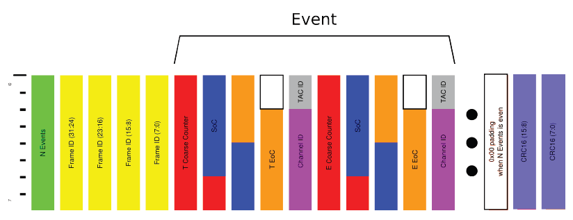
Figure 4
Data frame format (full event data). Each event includes time counters and channel ID (6-bit tag of the channel that generates the data). A 2-bit TAC ID records the index of the TAC used for a particular event.