PETsys TOFPET2 ASIC
The PETsys TOFPET2 ASIC is a high-performance 64-channel chip designed for readout and digitization of fast photon detector signals in applications requiring exceptional timing resolution and high data throughput.
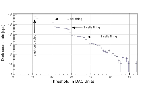
Each channel features dual processing paths optimized for timing and energy measurement. The timing branch uses an ultra-low threshold (t1), typically set to detect just a few photons, enabling precise time measurement. A secondary threshold (t2) rejects dark counts without introducing dead-time. The energy branch employs a higher validation threshold (tE), ensuring only genuine events are digitized. All thresholds are independently configurable per channel.
Four Time-to-Amplitude Converters and four Charge Integrators per branch enable high event rates with negligible dead-time. Energy measurement supports both charge integration (up to 2 μs) and Time-over-Threshold methods. Two 10-bit Wilkinson ADCs per channel provide complete digital event records, while embedded counters track dark counts for SiPM characterization.

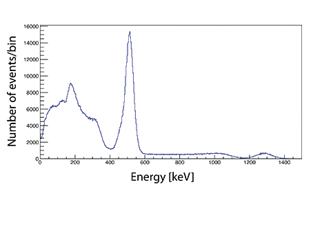 Pulse charge spectrum obtained with a source of 22Na and with a LYSO mounted on an SIPM, after external linerisation. The charge signal is integrated in a time window of 350ns. The energy resolution at 511 keV is 10.5%.
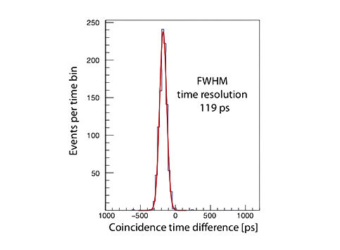 Time difference between the two signals from a positron annihilation event. Measured at 15°C with a 22Na point source and two 2x2x3 mm3 LYSO:Ce crystals coupled to two Hamamatsu S13361-3050AE MPPC arrays.
Main Features
- Designed in standard CMOS 110 nm technology.
- Signal amplification and discrimination for each of 64 independent channels.
- Dual branch analogue interpolation TDCs for each channel. The first branch is used for timing measurement. The second branch can either be used for time-over-threshold (ToT) or charge measurement (ADC).
- Quad-buffered charge integration for each TDC or ADC in each channel
- Dynamic range: 1500 pC.
- SNR 25 dB for Qin=200 fC (about one p. e.) and input capacitance of 320 pF.
- TDC time binning: 30 ps.
- Gain adjustment per channel: 1, 1/2, 1/4, 1/8.
- On-chip calibration pulse generator with 6-bit programmable amplitude.
- Max channel hit rate: 600 kHz.
- Rejects dark counts without triggering, allowing to handle over 1 MHz of dark counts.
- Separately configurable thresholds for each channel.
- Configurable charge integration time up to two microseconds.
- Fully digital output, 4 LVDS data links double data rate (DDR) compatible.
- Max output data rate: 3.2 Gb/s.
- Clock frequency: 200 MHz.
- Power consumption per channel: 8.2 mW, depending on certain settings